The DDS board
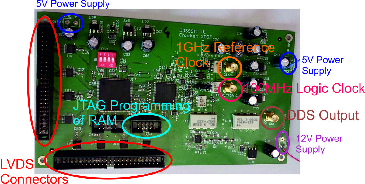
LVDS connectors
They are used to program the DDS output from the FPGA on the main board. Each DDS needs to have a different number on the bus. The number set at the DIP-Switch, the red box with the 4 switches, represents the number on the bus and is therefore important for programming the DDS output frequency. 5V Power Supplies and 12V Power
Supply
These have to be connected with the 5V, or respectively the 12V, power supply of the pulse box. The current consumption of a DDS board at normal operation can be estimated with about 1A.
Unfortunately, the holes at too small to use standard connectors for theses. Hence, it’s the easiest thing to directly solder the wires to the pads. But make sure that when you mount the DDS board, there is no stress on the cable. Otherwise the cable might break after some time, and checking each power supply of every DDS board is probably to first thing one might do when looking for the bug. 1GHz Reference Clock
This is the input of the reference clock signal, and its frequency has to be 1GHz. This frequency is supplied by the Clock Generator Board, or the Clock Distributor Board respectively. 100MHz Logic Clock
This is the input clock for the logic system on the board, and its frequency has to 100MHz. This frequency is supplied by the Clock Generator Board, or the Clock Distributor Board respectively, too.
DDS Output
This is the output connector of the generated frequency. Unfortunately, this output is not galvanicly isolated. Hence, in order to galvanicly isolate all pulse box outputs, one needs to add a transformer between the DDS output and the actual pulse box output.
Programming the FPGA
The FPGA on the DDS board can be programmed with two different protocols:
- JTAG - Temporary programming - Connector J1
- Active serial programming - Permanent programming - Conenctor J2
The JTAG port is used to convert the FPGA into a logic analyzer to test the LVDS bus. The permanent program of the FPGA is programmed via active serial programming. The firmware can be downloaded from the project homepage:
http://sourceforge.net/projects/pulse-sequencer/files/ad9910_firmware/RC1/
Troubleshooting
If the DDS gives a slightly wrong frequency (e.g. 100MHz instead of 80MHz) then the reference frequency in the software is set incorrectly.
If the DDS does not react at all, the LVDS bus needs to be investigated.