Introduction to the PBox
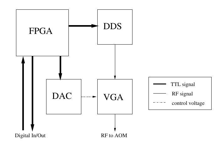
Basic working principle
The controls in an experiment are divided into synchronous and asynchronous signals.
| Synchronous | Deterministcally switched in one experiment cycle |
| Asynchronous | Switched between two experiments (may be varied in a scan) |
The Box is responsible for all synchronous signals in the experiment but can also generate asynchronous signals. The signal can be either digital (3.3V TTL) or analog radio frequency (RF) pulses. It features a special purpose micro-controller realized in an field programmable gate array (FPGA). This FPGA generates the digital signal and controls the direct digital synthesizers (DDS) that generate the RF pulses. The FPGA is connected to the experimental control computer (PC) with a standard ethernet connection.
Software wise, the PBox is controlled by a program called “sequencer2”. It is written in the python programming language. Note that a running sequencer2 version is required to perform the basic testing of the PBox hardware.
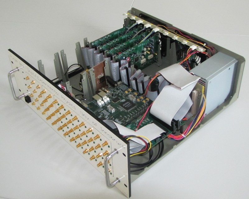
Overview over the Hardware
The new version of the PBox is built up from 5 main components:
| Mainboard | The main FPGA and the network connection |
| Synthesizer board | Auxiliary FPGA and DDS |
| Breakout board | Logic level converter and connectors |
| Digital IO board | Galvanically isolated connectors |
| Clock generator | Synchronizing all parts |
Which version of the Box do I have?
There exist two versions of the PBox. Their main difference that they use different RF-generation hardware (DDS). The mainboard is identical in hardware and firmware.
The versions can be distinguished by checking the DDS PCB boards. The old version uses an analog devices evaluation baord which has a blue PCB. The new version uses custom made DDS boards with a green PCB.
In general, the distinction can be made by looking at the cases. An image of the new version: